TSMC's role in the global AI and geopolitical order - a Full Report
Why I'm calling TSMC the most important tech company in the world for the future of AI. Severe trade tariffs but TSMC's role in the future of AI in the spotlight.
Welcome back,
Today we have a guest post from the foremost experts on TSMC writing on Substack, Semi Vision, currently ranked 12th in trending rising Newsletters in tech on the in-app leaderboard.
Introducing SEMI VISION
Their paid tier is $25 a month, fairly normal for their specialized research and area of expertise.
The report today is titled “TSMC in Strategic Focus: U.S. Expansion, Potential Intel Collaboration, and Navigating U.S.-China Tech Tensions”.
Why TSMC is so Crucial to the future of AI
As the U.S. vs. China trade war escalates the true “picks and shovels” company for AI Supremacy isn’t Nvidia, it’s TSMC. Taiwan Semiconductor Manufacturing Company (TSMC) has committed a total investment of approximately $165 billion in the United States complicating the geopolitical future in the era of reciprocal trade tariff uncertainty.
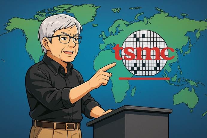
TSMC is the most important tech company in the world in 2025.
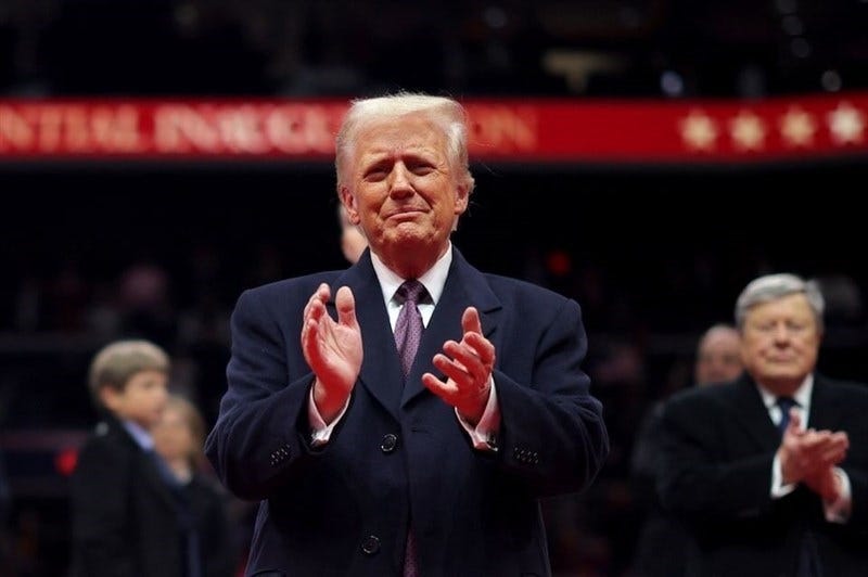
Under the Trump Administration, TSMC has promised epic expansions in Arizona, exasperated by tariff threats TSMC had no choice but to capitulate to Trump. The U.S. needs TSMC to stay competitive in national defense and AI, while TSMC could be on the verge of becoming the most important company in the world as it leads its rivals into unprecedentedly small and efficient semiconductor chips critical for the future of AI.
A threat to the island nation of Taiwan (e.g. like a blockade or invasion) and supply-chains of TSMC, would immediately plunge the global economy into a severe recession. It would also likely spark a hot war involving the U.S., Japan and other allies. The Trump administration appears to be escalating the situation:
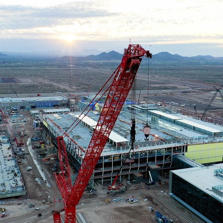
With the threats of tariffs, TSMC’s further investment in Arizona could mean this area becomes a center for the advanced technology to power artificial intelligence, sophisticated military systems, computers, electric vehicles and cellphones with a massive planned addition to a semiconductor complex in north Phoenix.
While revenue continues to surge at TSMC, Trump’s threat of tariffs on semiconductors and significant tariffs on Taiwan, have forced the island nation to make investments it may not easily be able to keep.
It’s Complicated
Many market analysts have raised concerns that much higher production costs in the U.S. will erode TSMC's profit margin and affect its cash dividend payout. According to Bloomberg, TSMC is warning of its inability to keep its chips outside of China. Meanwhile Huawei plans to begin mass shipments of its own advanced AI chip — the 910C — as early as next month, a supposed replacement for Nvidia’s H20 chips. On April 15th, Nvidia said that it will take a quarterly charge of about $5.5 billion tied to exporting H20 graphics processing units to China and other destination since on April 9, the U.S. government told Nvidia it would require a license to export the chips to China and a handful of other countries.
The Semiconductor Stock Crash of 2025
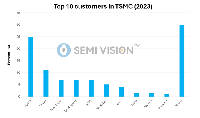
On the stock market, the semiconductor stocks are imploding as of April, 2025. Nvidia is down 30% and TSMC is down nearly 27% so far this year with the entire sector in turmoil, but the worst may be still yet to come for investors. TSMC’s biggest customers are the likes of Nvidia, Apple, AMD, Qualcomm, Broadcom and others. There are many good reasons I’m calling TSMC the most important tech company in the world.
I hope this report sheds important details on why this is the case in this peculiar geopolitical uncertainty around the U.S. vs. China, export controls and the critical future of the semiconductor industry. In my Newsletter Semiconductor Things, I delve into the news cycle around this industry.
At this point I’ll turn it over to the experts:
What is SemiVision Newsletter?
SemiVision is a semiconductor industry research institution committed to transforming analysis into vision through comprehensive insights into the semiconductor ecosystem. The semiconductor industry’s future is shaped by cutting-edge innovations such as AI, silicon photonics, advanced packaging, and more. At the heart of this ecosystem lies the interplay between foundries, semiconductor manufacturing, fabless design houses, and ASIC (Application-Specific Integrated Circuit) development—each a critical pillar supporting the chips and technologies that power our world.
SV Works:
I consider SemiVision critical reading for investors, China watchers, U.S. AI policy types and analysts in the Semiconductor space as of 2025, among others.
NVIDIA x TSMC: A Milestone in Silicon Photonics and Optical Integration
How TSMC’s Silicon Photonics Could Impact NVIDIA’s Future
2025 GTC Review: The Silicon Photonics Era Has Arrived – Get Ready!
The Rise of ASIC: Custom Chips Becoming a Key Trend!
SemiVision is the fastest growing paid semiconductor Newsletter on Substack as of early 2025.
By Jett and Eddy, March, 2025 via SEMI VISION_TW
The State of TSMC in the Global Order: Report
TSMC in Strategic Focus: U.S. Expansion, Potential Intel Collaboration, and Navigating U.S.-China Tech Tensions
As global semiconductor dynamics are increasingly shaped by geopolitics, Taiwan Semiconductor Manufacturing Company (TSMC) finds itself not only at the forefront of technological innovation but also at the very center of a high-stakes geopolitical chessboard. Amid intensifying U.S.-China tech rivalry and a global push to localize supply chains, TSMC’s strategic decisions—from its multibillion-dollar investment in Arizona, to its rumored advanced packaging collaboration with Intel, to its response to political pressures from Washington—are reshaping the semiconductor landscape and influencing the global balance of technology power.
This article offers a deep dive into TSMC’s current strategic positioning through five key lenses: (1) the scope and implications of its U.S. capacity expansion and how it manages geopolitical risks; (2) the potential cooperation model with Intel on advanced packaging or shared manufacturing capacity; (3) the increasing pressure from the U.S. government regarding transparency, capacity allocation, and alignment with national interests; (4) its financial performance and capital expenditure outlook amid global uncertainty; and (5) the status and competitive edge of its 2nm and sub-2nm process technology roadmap. Together, these dimensions reveal not only the complexity of the challenges facing TSMC, but also the resilience and adaptability required for it to sustain its leadership role in an evolving and fragmented global semiconductor supply chain.
This report is the most in-depth report on TSMC I have personally read. A good read for investors, China watchers, U.S. policy experts, venture capital talent and semiconductor workers at large.
It breaks down the most important details in the U.S.-China and U.S-Taiwan implications in tariffs and trade considerations.
The report goes into unprecedented details about why TSMC is so important in the global order from and by experts in located in Taiwan itself.
I. Introduction: A Technological Leader and a Geostrategic Actor
Taiwan Semiconductor Manufacturing Company (TSMC) has long been the undisputed global leader in semiconductor foundry services. Its dominance is rooted in a powerful combination of cutting-edge process technologies, industry-leading yield control, massive production scale, and deep integration with key customers. This competitive moat has enabled TSMC to secure and sustain its leadership position—especially in advanced nodes critical to next-generation computing.
Yet in the current era, technical excellence alone is no longer sufficient. As global tensions escalate and countries prioritize “de-risking” their supply chains, semiconductors have evolved from commercial products into strategic national assets. In this context, TSMC has been thrust to center stage—not only as an industrial powerhouse but as a pivotal player in the unfolding geopolitical realignment.
In 2024, as AI-driven workloads surge, capital investments shift toward advanced manufacturing, and U.S.-China technological rivalry continues to intensify, TSMC stands at the crossroads of technological innovation and strategic transformation. Every capital expenditure, fabrication site decision, and international partnership it undertakes now carries global implications for semiconductor supply chain resilience and security.
As the supplier behind over 90% of the world’s advanced-node (under 18nm) semiconductor manufacturing, TSMC is indispensable to mobile SoCs, AI accelerators, and high-performance server platforms. Its influence is also expanding into defense, autonomous vehicles, and critical cloud infrastructure. What was once primarily a matter of technical leadership has now become a symbol of trust, strategic leverage, and geopolitical balance in the global technology order.
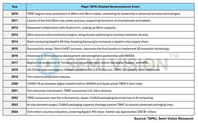
Since the outbreak of the U.S.-China trade war in 2018, the global semiconductor landscape has undergone dramatic shifts—with TSMC emerging as a central figure in the geopolitics of technology. As the U.S. imposed sweeping export controls on Chinese tech firms and nations worldwide accelerated efforts to localize chip production, the global supply chain entered a period of accelerated restructuring. Amid this upheaval, TSMC not only maintained its leadership but achieved significant breakthroughs in both technology and market capitalization. At its peak, TSMC’s valuation surpassed $600 billion, making it one of the most valuable technology companies in Asia and a bellwether of global semiconductor performance.
This section explores the three key forces behind TSMC’s remarkable growth trajectory—analyzing the turning points in its market capitalization, the structural drivers of its sustained advantage, and its strategic resilience in adapting to future disruptions.
Three Core Growth Drivers
1. Technological Leadership: Global Domination in 7nm, 5nm, and 3nm Nodes
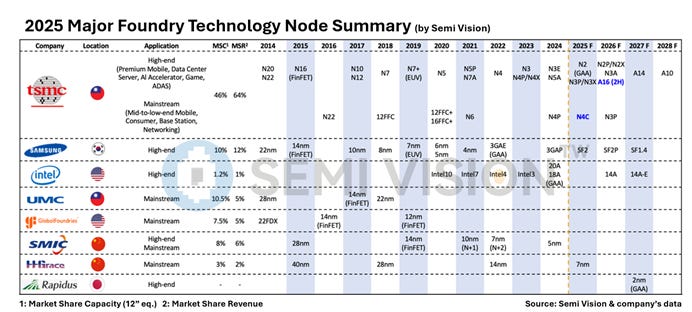
TSMC has built its long-standing lead by consistently advancing its process technology roadmap. Its 7nm node marked a major inflection point, while the 5nm process became the foundation for next-generation chips from Apple, NVIDIA, AMD, and others. With the 3nm (N3) node, TSMC became the first foundry to commercially scale a gate-all-around (GAA) transistor architecture. By 2024, TSMC controls over 90% of the global sub-7nm foundry market, creating both a technical and capacity monopoly. This dominance makes TSMC indispensable for high-end computing, smartphone SoCs, and AI accelerators—driving robust revenue growth and industry-leading gross margins. Crucially, it also reinforces “technological lock-in” with its customers, turning TSMC into a high-barrier strategic asset in the eyes of global investors.
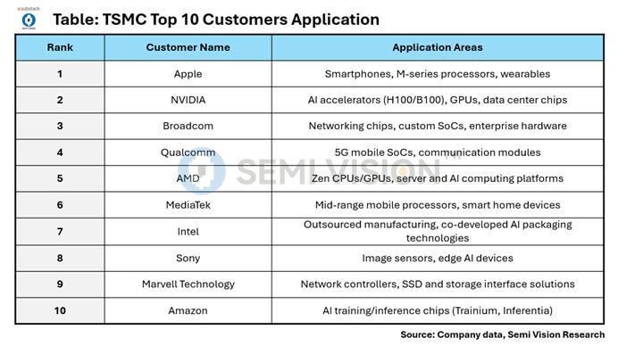
TSMC remains the only semiconductor foundry in the world capable of reliably and consistently mass-producing advanced process nodes below 7 nanometers. Since the introduction of 7nm, the company has outperformed all competitors in yield optimization, cost control, and time-to-volume execution—positioning itself as the foundry of choice for the world’s most demanding semiconductor clients. These include Apple’s A-series and M-series processors, NVIDIA’s H100 and GH200 AI accelerators, and AMD’s Zen-based CPUs. This form of manufacturing monopoly at the leading edge has enabled TSMC to generate exceptional profit margins and exert significant pricing power within the global foundry market. As a result, TSMC not only holds a dominant position in AI, high-performance computing, and mobile SoCs, but is also increasingly viewed by global investors as a strategic, irreplaceable asset within the semiconductor value chain.
2. Explosive Growth in AI and High-Performance Computing (HPC) Demand
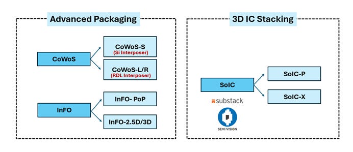
The rapid proliferation of generative AI models, edge computing, and next-generation wireless technologies such as 5G and 6G has triggered a global surge in demand for high-performance semiconductor solutions. From large-scale cloud GPUs to edge AI SoCs, virtually every advanced computing workload today relies on TSMC’s leading-edge process technologies and advanced packaging capabilities. Key customers include global tech giants such as NVIDIA, Google, Meta, and Amazon. TSMC’s leadership in advanced packaging—particularly in CoWoS, InFO, and SoIC—positions it as the dominant provider for high-bandwidth memory (HBM) stacking and large-area AI chips, cementing its role at the heart of the global AI/HPC ecosystem.
3. Strategic Neutrality and Supply Chain Trust in a Geopolitical World
Amid escalating U.S.-China tech rivalry and broader geopolitical uncertainty, semiconductor buyers are increasingly prioritizing not only technical performance, but also supply chain resilience and political neutrality. TSMC’s unique position as a “non-China, non-U.S.” supplier gives it a rare form of geopolitical trust, making it the foundry of choice for multinational tech firms seeking dependable long-term supply. From U.S. CHIPS Act subsidies for its Arizona fabs, to invitations from Japan and the EU to establish local production, TSMC is now a centerpiece of national semiconductor strategies across multiple regions—transforming geopolitical pressure into global opportunity.
Outlook: From Process Leader to Infrastructure Backbone for AI
By 2025, TSMC is expected to begin mass production of its 2nm node featuring gate-all-around (GAA) transistor architecture. It is also advancing its next-generation back-end integration capabilities to meet the extreme bandwidth and efficiency demands of upcoming AI platforms such as NVIDIA’s GB200 and AMD’s MI400. Furthermore, TSMC’s investment in photonic integration—particularly in co-packaged optics (CPO) and Optical I/O—signals its ambition to become a core enabler of next-gen AI system architectures. If TSMC can drive ecosystem-wide upgrades while overcoming challenges in cost and thermal performance, it will evolve beyond foundry leadership to become a global infrastructure pillar for AI computing.
R&D Investment Strategy
To safeguard its long-term competitiveness and innovation capacity, TSMC continues to aggressively invest in research and development:
· Over $6 billion in R&D expenditure in 2023, accounting for nearly 9% of total revenue.
· Focus areas include GAA transistor development, 3D IC integration, and silicon photonics platform technologies.
· Geographic diversification of innovation hubs: expanding R&D and manufacturing presence in Arizona (U.S.), Kumamoto (Japan), and Dresden (Germany) to enhance global supply chain stability and regional trust.
II. U.S. Expansion: Strategic Move or Political Response?
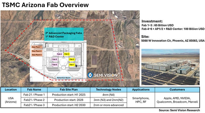
TSMC has committed over $65 billion USD to the phased construction of three advanced semiconductor fabs in Arizona, targeting 4nm, 3nm, and upcoming 2nm process nodes. This initiative marks the company’s largest overseas manufacturing investment to date. In early March 2024, TSMC CEO C.C. Wei led a delegation to the White House, where he announced an additional $35 billion in investments, bringing the total to $100 billion. This expanded plan includes three more fabs, a dedicated R&D center, and two advanced packaging facilities—signaling a major escalation of TSMC’s localization strategy in the United States.
While TSMC officially attributes this expansion to customer demand and the need to strengthen supply chain resilience through geographic diversification, many observers interpret the move as being heavily influenced by political pressure from the U.S. government. Under both the Trump and Biden administrations, Washington has encouraged—or compelled—strategic reshoring of semiconductor manufacturing. From “Made in America” policies to the CHIPS and Science Act’s incentive packages and national security clauses, the U.S. has created both carrots and sticks to guide corporate decisions.
In this light, TSMC’s Arizona investment reflects not only a calculated global strategy but also a response to intensifying geopolitical pressure. It underscores the company’s delicate position at the intersection of supply chain neutrality, customer alignment, and sovereign state interests—balancing innovation leadership with the growing weight of political expectations in an era of tech sovereignty.
Since 2020, TSMC’s presence in the United States has rapidly evolved from a single production site to a comprehensive semiconductor ecosystem encompassing advanced fabrication, heterogeneous packaging, and front-end R&D. This strategic expansion aligns with the U.S. CHIPS and Science Act’s push for domestic advanced-node capabilities and signals TSMC’s ambition to consolidate its leadership in the global AI-driven semiconductor supply chain.
TSMC’s U.S. Expansion Blueprint (2020–2025): From Manufacturing to Innovation Hub for the AI Era
Since 2020, TSMC’s presence in the United States has rapidly evolved from a single production site to a comprehensive semiconductor ecosystem encompassing advanced fabrication, heterogeneous packaging, and front-end R&D. This strategic expansion aligns with the U.S. CHIPS and Science Act’s push for domestic advanced-node capabilities and signals TSMC’s ambition to consolidate its leadership in the global AI-driven semiconductor supply chain.
Key Milestones and Investment Timeline:
May 2020: Initial U.S. Fab Announcement
• TSMC announces a $12 billion investment to build its first U.S. fab (Fab 21) in Phoenix, Arizona, targeting 5nm production with an expected monthly capacity of 20,000 wafers.
• Context: A direct response to U.S.-China trade tensions and Washington’s strategic push to localize advanced semiconductor manufacturing.
December 2022: Investment Rises to $40 Billion
• TSMC commits to a second fab (Fab 22), introducing 3nm production. The total investment rises to $40 billion, marking the largest foreign manufacturing investment in U.S. history.
• Impact: Combined facilities expected to employ over 4,500 high-tech workers, signaling a permanent shift toward U.S.-based advanced chip production.
April 2024: U.S. Funding Secured + Third Fab Planned
• The U.S. Department of Commerce awards:
– $6.6 billion in grants
– Up to $5 billion in low-interest loans
• Funds will support construction of a third fab featuring 2nm node technologies, increasing the total committed investment to $65 billion.
March 2025: Massive Expansion to $165 Billion Including R&D
• TSMC announces an additional $100 billion in new investment, bringing the total to $165 billion.
• Expanded scope includes:
– Three fabs (5nm / 3nm / 2nm)
– Two advanced packaging facilities (CoWoS, SoIC-ready)
– One U.S.-based R&D center
Strategic Role of the R&D Center: From Localization to Innovation Leadership
The R&D center represents TSMC’s first full-scale research hub in the U.S.—marking a shift from manufacturing localization to frontline innovation. The center will focus on:
· Next-generation process nodes (including GAA and sub-2nm scaling)
· 3D IC integration and packaging (CoWoS, SoIC)
· Specialized AI chip materials, electrical simulation, and signal integrity testing platforms
· Silicon photonics and co-packaged optics (CPO) process development
This initiative is expected to deepen collaboration with leading U.S.-based chip designers such as NVIDIA, AMD, and Google—fostering a joint innovation model that integrates architecture and process R&D, accelerating the co-evolution of AI system performance and semiconductor manufacturing capabilities.
Geopolitics and Supply Chain Risk Management: From Pressure to Strategic Repositioning
Amid rising geopolitical tensions and the global trend toward technological sovereignty, TSMC’s U.S. expansion has become more than a matter of capacity—it is a deliberate response to supply chain security and policy-induced risk.
• U.S. Political Pressure Revealed: In 2025, former President Donald Trump publicly stated that his administration had explicitly pressured TSMC to build a fab in the U.S., warning that failure to comply could result in 100% punitive tariffs on its products. This underscores how TSMC’s Arizona investment was shaped not only by market logic, but also by strategic coercion—reflecting Washington’s view of advanced semiconductors as national security assets.
• Clarification from China on Tariffs: Also in 2025, the China Semiconductor Industry Association (CSIA) issued a statement clarifying that U.S.-designed, Taiwan-manufactured chips would continue to be recognized as Taiwan-origin goods—thus exempt from China’s retaliatory tariffs. This helped reassure global customers and highlighted TSMC’s rare value as a geopolitically neutral supplier in an increasingly fragmented world.
Arizona’s Fab 21 Enters Mass Production: A Dual Milestone in Technology and Strategy
In April 2025, TSMC’s first Arizona fab—Fab 21—officially entered mass production of 4nm chips, marking a watershed moment for U.S.-based advanced semiconductor manufacturing. For TSMC, this milestone validates its localization strategy. For the U.S., it represents the tangible return of cutting-edge chip production to American soil.
Conclusion: The U.S. as TSMC’s Next Global Strategic Stronghold
TSMC’s U.S. operations have evolved into a strategic semiconductor campus spanning leading-edge fabrication, advanced packaging, and front-end R&D. While the project reinforces U.S. ambitions for semiconductor autonomy and AI infrastructure, it also elevates TSMC’s geopolitical importance on the world stage. However, this transformation comes with three major challenges:
1. High Production Costs: Building and operating fabs in the U.S. is estimated to cost 2–3x more than in Taiwan, pressuring profitability.
2. Talent and Experience Gaps: U.S. engineers lack deep experience in volume chip manufacturing, requiring extensive training and cultural adaptation.
3. Immature Supply Ecosystem: The U.S. still lacks the dense, mature supplier networks—especially in EUV tool maintenance, advanced material logistics, and spare parts delivery—that make TSMC’s Taiwan operations so efficient.
Another major challenge lies in establishing long-term trust with U.S. government agencies, local authorities, and labor unions, while maintaining tight control over process secrecy and ensuring cultural alignment across regions.
Nonetheless, the strategic value of the U.S. market—and its strong political will to revive domestic chip production—has made this investment an inescapable move for TSMC. It now serves not only as a manufacturing site, but as a geopolitical hedge and possibly a bargaining lever in future dialogues with China.
III. TSMC × Intel: Strategic Collaboration Amid Competition?
Recent industry buzz suggests that TSMC and Intel are in advanced discussions on multiple fronts—including wafer foundry outsourcing, advanced packaging integration, and potentially the formation of a joint venture. The collaboration may combine Intel’s leading-edge designs with TSMC’s CoWoS packaging technology, creating a powerful alliance that carries dual strategic significance:
On one hand, Intel, as a traditional IDM leader, is under pressure due to yield and timeline challenges in its latest process nodes. Outsourcing to TSMC enables it to maintain volume ramp-up for products like AI accelerators and data center chips. On the other hand, TSMC benefits from expanding its influence on U.S. soil, while reinforcing ties with American customers and policymakers—a crucial balancing act in the age of supply chain politics.
Customer Co-Investment Model: Consistency Across the U.S. and Europe
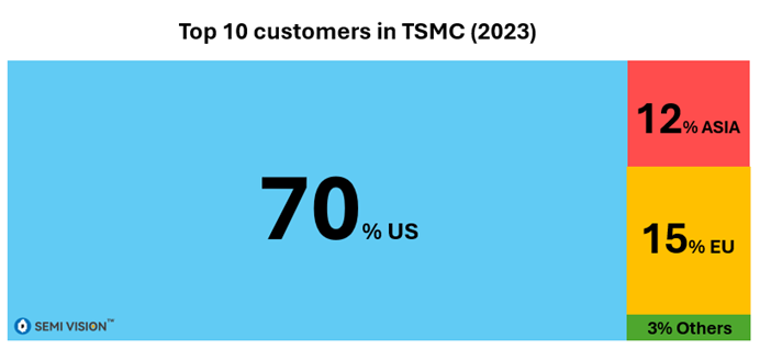
In Arizona, TSMC’s major customers—NVIDIA, AMD, Apple, Broadcom, Marvell, Qualcomm, and Intel—have strong stakes in securing advanced node capacity. Reports suggest that some of these firms have participated in fab development via financial contributions, tool commitments, or technical collaboration. This co-investment model helps mitigate upfront CAPEX, while ensuring preferential capacity and closer supplier alignment.
TSMC is replicating this model in Europe as well, most notably in its new Dresden fab project, where Bosch, Infineon, and NXP are partners in a joint venture. This illustrates TSMC’s modular approach to global expansion, blending localization with strategic customer integration.
Technology Leakage Concerns: Different Design Rules, Complementary Strengths
Some in Taiwan have expressed concerns about potential technology leakage from partnering with Intel. However, it’s important to note that Intel and TSMC operate under entirely different design rules. Their process flows, toolchains, and PPA optimization strategies are fundamentally incompatible.
For example, Intel’s upcoming 18A process is expected to enter volume production soon. TSMC internally categorizes it as functionally equivalent to its own A16 node, suggesting technical parity rather than superiority or dependency. Intel’s challenges lie not in technology, but in execution and manufacturing efficiency. Thus, the collaboration is better understood as a complement of manufacturing capabilities, not a transfer of proprietary process IP.
Advanced Packaging and UCIe: Enabling a Modular Chip Ecosystem
For TSMC, this partnership would reinforce its global leadership in advanced packaging. As chiplet architectures and 3D stacking become central to modern chip design, packaging has become a frontline enabler of system performance, power efficiency, and integration flexibility.
Should TSMC and Intel collaborate on open packaging standards such as UCIe, they could accelerate industry-wide adoption of modular, interoperable architectures, making it easier to assemble complex SoCs from diverse components. This could lead to a new wave of composable hardware innovation, bridging chip manufacturing with system-level design freedom.
Still, questions remain: Will this change the long-term competitive dynamics? Intel remains a potential rival in advanced foundry services. Whether this collaboration helps Intel rebuild its manufacturing credibility and ultimately compete for TSMC’s top-tier customers remains a closely watched development.
IV. Political Pressure and the U.S.–China Trade Shadow: Strategic Balancing in a Bipolar Tech World
TSMC’s globalization strategy is increasingly shaped by geopolitical pressure between the U.S. and China. During the Trump administration, the imposition of punitive tariffs and the expansion of the U.S. Entity List blurred the definitions of chip origin and compliance—impacting TSMC’s client structure and shipment flexibility.
Media reports revealed that Trump warned TSMC directly: “If you don’t build fabs in the U.S., your chips will face 100% tariffs.” This public pressure illustrated how TSMC’s U.S. investment decisions were not purely market-driven, but influenced by the necessity to balance economic logic with sovereign coercion.
Despite China remaining a critical market—especially in mobile and consumer electronics—rising geopolitical risk has accelerated TSMC’s diversification of markets and capacity.
Incentives and Pressure: The Dual Nature of the CHIPS Act
The U.S. CHIPS and Science Act offers substantial subsidies to lure semiconductor manufacturing back to American soil. For TSMC, this creates a landscape where government incentives come bundled with structural obligations:
· In the short term, these subsidies help offset high capital expenditures and ease financial burdens.
· In the long term, however, TSMC must navigate challenges related to labor shortages, cultural adaptation, union negotiations, and potential policy volatility—especially if political leadership changes.
Strategic Neutrality in Action: Global Manufacturing as Geopolitical Hedging
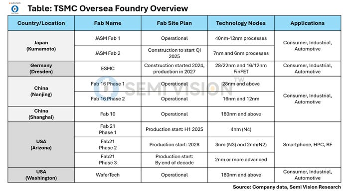
TSMC is clearly shifting toward a multi-region manufacturing model to reduce dependency on any single market. This “neutralization strategy” is evident in its investment footprint across Asia, North America, and Europe, building a multi-tiered network for resilience, technology leadership, and regional relevance:
· Taiwan remains the technological and operational heart, with fabs for 5nm, 3nm, and future 2nm nodes, plus advanced packaging (CoWoS, SoIC).
· Arizona, USA is the North American anchor, with $165 billion invested across 3 fabs, 2 advanced packaging facilities, and 1 R&D center, serving customers like NVIDIA, Apple, AMD, and Intel.
· Kumamoto, Japan (JASM): Joint venture with Sony and Denso, with the first 22/28nm fab set for mass production in late 2024 and a second fab planned with more advanced nodes.
· Dresden, Germany (ESMC): Joint venture with Bosch, Infineon, and NXP, focused on 28nm and mature nodes for automotive and industrial markets.
· China (Shanghai & Nanjing): Operating 8-inch and 12-inch fabs at 16/28nm nodes for local market demand.
· Global R&D & Support Centers: Established in Yokohama, Tsukuba, and Arizona, focused on 3D IC, silicon photonics, and heterogeneous integration.
Conclusion: Building Resilience Amid Political Crossfire
In an era of entrenched U.S.–China tech rivalry, TSMC’s global expansion is more than business strategy—it is a geopolitical risk mitigation framework. Through cross-regional manufacturing, diversified packaging, and international collaboration, TSMC is not only safeguarding its leadership in AI, HPC, and automotive semiconductors, but also positioning itself as a neutral, indispensable backbone of the future technology ecosystem.
V. Financial Performance & Revenue Outlook: AI as the Primary Growth Engine
According to TSMC’s financial disclosures for 2023 and 2024, Artificial Intelligence (AI) and High-Performance Computing (HPC) have emerged as the company’s primary growth drivers. In Q1 2025 alone, TSMC reported consolidated revenue of NT$839.2 billion, representing a 41.6% year-over-year increase, with gross margin remaining above 52%. The company expects $25–30 billion USD in capital expenditures this year, primarily allocated to 3nm node and CoWoS packaging capacity expansion.
By 2024, AI-related workloads and HPC applications have become core contributors to TSMC’s growth. CoWoS capacity is fully booked, and hyperscalers such as NVIDIA, Google, and Amazon rely almost exclusively on TSMC for their advanced AI chip production
Looking Ahead: Dual Engines of Growth
In addition to AI and HPC, rising demand for automotive electronics, 800G/1.6T networking, and enterprise SSD controllers is fueling steady growth in mature nodes like 16nm and 28nm. This balance of high-margin advanced nodes and cash-generative mature processes provides a stable financial foundation for TSMC’s ongoing capital investment and R&D acceleration.
These customers primarily span critical sectors including AI and high-performance computing (HPC), smartphones, telecommunications infrastructure, and cloud platforms, underscoring TSMC’s global leadership in advanced process nodes (e.g., 3nm, 5nm) and cutting-edge packaging technologies (e.g., CoWoS).
Editor’s Notes
SemiVision is a semiconductor industry research institution committed to transforming analysis into vision through comprehensive insights into the semiconductor ecosystem.
Read more on SEMI VISION Newsletter. For daily commentary please see Jett Chen’s LinkedIn posts. As of today April 22nd, 2025 it’s the #12 ranked rising in Technology Newsletter, a significant achievement for a relatively new Newsletter out of Taiwan.
It makes sense that many of the top semiconductor Newsletters are repotted from Taiwan, the most important country (by far) in the world for this area of technology.
A special thanks to Judy Lin 林昭儀 of TechSoda Newsletter for her help, another notable journalist who is a highly esteemed TSMC watcher.
A failure of export controls
TSMC has warned of its limits in keeping its AI chips from reaching China. Earlier an investigation by Canada-based research firm TechInsights last year showed that Huawei’s Ascend 910B AI chip contained semiconductors by TSMC. The U.S. department of commerce could fine TSMC, according to reuters. TSMC does its best to abide by export restrictions but various third parties are not in its control. The chipmaker halted shipments to a client at about the same time after it found out the semiconductors it made for the customer ended up with Huawei.
If you want to follow the semiconductor industry and TSMC news in particular diligently, finding the right Taiwanese based publications and Newsletters is critical.
TSMC provides manufacturing services to many so-called fabless firms and chip designers, including Nvidia.
A stock market in turmoil, especially tech stocks
TSM 0.00%↑ TSMC’s stock is down 18% in the past month due to trade war and the Trump administration’s reckless uncertainty around tariffs, the independence of the Federal Reserve and other related issues and topics beyond the control of TSMC.
The NASDAQ 100 is down an usual 15% so far in 2025 due to the Trump Administration’s bizarre policies and stunning reciprocal tariff war on the world, including allies. Many fear these U.S. policies are leading to a self-fulfilling prophecy of a U.S. recession beginning near the end of 2025.
I hope this report has given you added context on the incredibly important role of TSMC, Taiwan and the semiconductor supply-chain to the future of AI.






Check out the Notes of SemiVision to keep up in touch with important updates about the Semiconductor industry and especially TSMC: https://tspasemiconductor.substack.com/notes
Snyk has a webinar coming up and they are one of my sponsors for May, 2025: check out the webinar: https://www.vpdae.com/redirect/qjcjlepcmyfonqxn2hten8mo3az